Whitepaper: Sharing PCB designs
Since the early Modular LED Displays more than 15 years ago, sharing custom-designed electronics has been an integral part of the development. When we combined more than 15 different repositories authored by various contributors into this website, the importance of having a consistent code and documentation quality became apparent. This document suggests how to achieve comparable coverage for printed circuit board (PCB) designs. This text’s suggestions are based on experience from organizing the different generations of the displays and are driven by the idea to “publish early, publish often.”
Please feel encouraged to share your modifications of the design by following the checklist. In case you want to know more details, we linked each checklist item with a more detailed description. Some of these sections contain links to “Further Readings” if you are looking for even more information. If you are unsure, please get in contact or submit the files through GitHub: a not-yet-perfect file is often more useful for others than a finished and polished version not yet released.
Checklist
We would appreciate the following files for each change. If you submit these files to us when you also send them to the PCB manufacturer and assembly houses, there should be almost no additional work required. If you want to send intermediate versions between hardware revisions, we can use the repositories to keep track of that, too.
- Schematic drawing (e.g.,
*.pdf) - PCB Design (e.g.,
*.brdfor Cadence or*.kicad_pcbfor KiCad) - Gerber files (e.g.,
*.artfor Cadence or*.gbrfor KiCad) - drill file (e.g.,
*.drlfor Cadence and KiCad) - Bill of Materials (e.g.,
*.csvor*.xlsx) - Invoice or price estimate (e.g.,
*.pdfor text) - Short description and file version this was based on
While the above files should be available for each hardware revision, some of the files below are nice-to-have, but not crucial. For the PCB manufacturers’ feedback, the actual form and schedule depend on external factors; some prefer to communicate through an online system, others favor email, and a few don’t give any feedback. Providing photos and renderings is intended to improve the documentation and are not crucial to producing the PCBs, but having them saves future time and effort with minimal initial work.
- placement file (e.g.,
*.txt) - feedback from PCB manufacturer
- Schematics Design (e.g.,
*.dsnfor Cadence and*.schKiCad) - suggestion for a version number
- alternative license
- rendering of boards (e.g.
*.jpgand*.png) - photo of produced board (e.g.
*.jpgand*.png) - suggestion for improving the documentation
EDA Design
Two different tool sets are being used to develop PCBs for the Modular LED Display, namely a software offered by the company “Cadence Design Systems” and KiCad. While most of the generated output files follow industry standards and are reasonably similar to each other, the design files (or “sources”) are not interchangeable between the two types specified above. Each set of a component’s design files are only available for one of the two tool sets, depending on who designed this particular module.
The company “Cadence Design Systems” offer different solutions for Electronic Design Automation (EDA) such as “Cadence Allegro” (Allegro for short) and “Cadence OrCAD” (OrCAD for short). To our understanding and according to our tests, either one of these commercial solutions can be used to modify design files such as *.brd. Therefore we use the term “Cadence” if either Allegro or OrCAD can be used. Before buying the software for this project, consult with the customer support what best suits your needs.
KiCad is an open source tool that can be licensed without cost.
If your submission is based on an existing version from the repository, please let us know which one you used. You can use the repositories to archive any design-related file, from project files such as the *.pro files for a KiCad project to component libraries. Please let us know if any of the files are not compatible with the currently used license.
Cadence and KiCad both divide the design process into a schematic design phase and a PCB design. Here a quick run through about which files would be interesting to share:
Schematic design
The focus of the repositories is on the production of Modular LED Displays and, therefore, the PCB design. Yet, to understand the PCB design, it is necessary to track changes in the schematics. Therefore some visualization of the schematic drawing should be provided every time something has changed. In the past, these schematics were shown through documents such as *.pdf files. Other image formats like *.png files are not ideal, but better than nothing.
Since schematic drawings are generated from schematic design files, it can help track the schematic designs in the repositories, too. Cadence, and more specific OrCAD uses *.dsn files. Recent versions of KiCad switched to *.kicad_sch file extensions while old versions use *.sch for the schematic design files. Some of the designs can consist of several schematic files or additional library files containing details for used electrical components. Please provide all files necessary for opening the schematic. As a user of your tool set, you probably know best which files are required.
The handover between the schematic design and the PCB design is, among others, a netlist file. Since the netlist can be generated from a valid schematic design file, it is unnecessary to keep track of these files in the repositories.
PCB design
The purpose of the repositories and documentation is to enable other labs to produce their own Modular LED Displays. Different PCB manufacturers and assemblers might require slightly different versions of the fabrication files. Therefore it is necessary to share the PCB design files so that these labs can generate fabrication files according to their assembly houses. At this time (2020), some PCB manufacturers also start accepting design files, for example, from KiCad to export the fabrication files in the exact format they need. So even if you decide not to share the schematic design files and only want to provide a schematic drawing instead, a shared PCB design file will make life easier for everyone.
PCBs for the Modular LED Displays were designed either with Cadence or KiCad. The design files for Cadence uses *.brd as a file extension while KiCad uses *.kicad_pcb at this stage. For example, the G4 panel driver starting with version 1, has been developed in Cadence while the panel communication board is being developed in KiCad. Consequently, the driver board’s repository is used to track the latest design iteration in the Cadence file format as a *.brd file as well as the latest design iteration in a KiCad file format that uses the extension *.kicad_pcb.
Some designs might require additional files; please make sure to share all files that are necessary to open the PCB design file. For example, footprints of other components can be in a *.kicad_mod file.
Further Readings
- CircuitHub: Taking the hard out of hardware: Explains how to upload native design files to the manufacturer and use their revision history system
Fabrication files
“Fabrication files” is a set of files sufficient to produce the PCBs. The EDA tools generate the files from the PCB design files. Although file types are, in general, defined by industry standards, there are small differences between PCB manufacturers and tools. Either Cadence tool as well as KiCad support different settings for each of the generated files. It would be tedious to explain the various options. Instead, we list some best practices that create something similar to the lowest common denominator and have proven to work so far. We hope to improve these descriptions over time.
Gerber files
Files in the Gerber format describe the different layers of a PCB in a vector format. By now, all PCB manufacturers can work with the “Extended Gerber format RS-274X”. The Gerber format is ASCII based, which is well suited to track changes through git. The standard file extension is *.grb, and KiCad produces such files through the File → Plot menu. Cadence generates RS-274X files with the extension *.art, which can easily be renamed – either on our side or the PCB manufacturers’ side.
Both tools generate one file per layer, for example, copper layers, the solder paste layers on front and back for surface-mount technology (SMT) boards, and the silkscreen. Some designs use additional files to describe the edge cuts or the application of adhesives. For a four-layer PCB, this can mean almost any number of Gerber files are produced, typically nine for an SMT board: 4×copper, front + back silkscreen, front + back solder paste, and edge cuts.
There is no standard for how the files are named. Therefore the PCB manufacturers require a description of the order of files and other parameters such as board thickness and distance between layers. This is either done through an additional file often called Assembly.art (for Cadence). This file contains a cross section chart that visualizes all layers in their respective order including their dielectric layers and layer thickness. KiCad on the other hand produces a human-readable JSON file with the extension *-job.gbrjob and the same information in text form. A standard that is currently developing and getting more widely accepted is the “Gerber Job” file format. Since there is no standard, make sure to check with your PCB manufacturer what format they accept.
OrCAD Gerber export
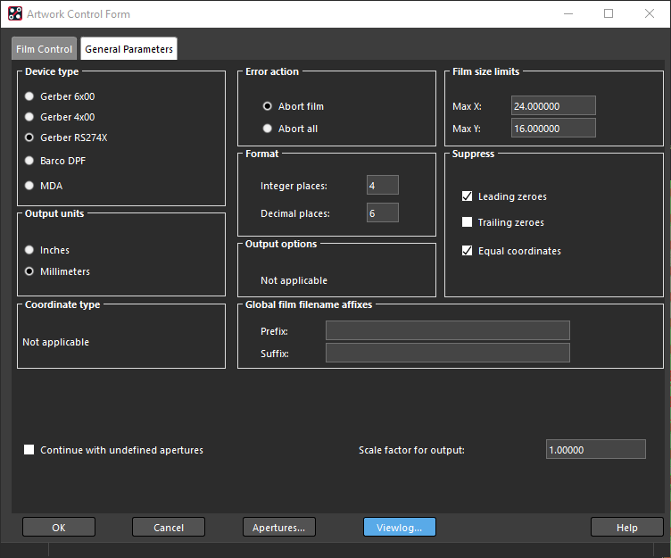
You need to set a few parameters to get a good quality gerber file. The screenshot is taken from Cadence OrCAD, but options in Cadence Allegro will look fairly similar. When you choose Export → Gerber, make sure to set the General Parameters as shown in the screenshot. Pay attention to the Device type which should be Gerber RS274X, to the Output units which should be Millimeters, and the Format, which should have 4 integer places and 6 decimal places.
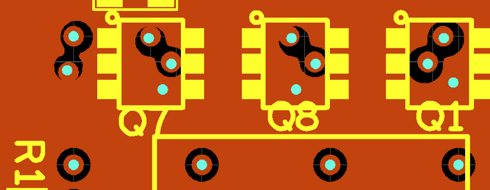
Especially not setting the precision in the format can lead to errors that are difficult to spot. The screenshot on the right shows vias that should be in the center of the plane cutouts, but due to a wrong format, some of them connect to the plane (while most don’t).
KiCad Gerber export
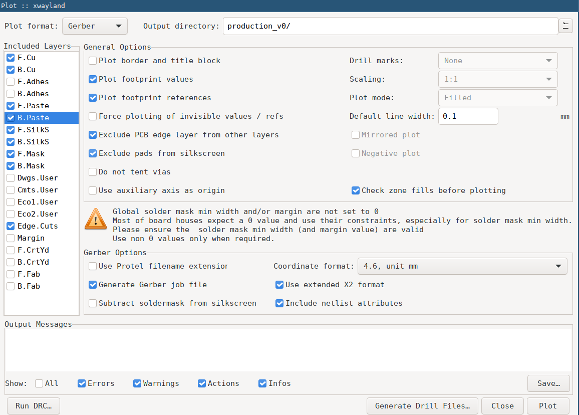
The screenshot shows which options have worked well in the past for KiCad. Note the coordinate format with units in mm and a precision of 4 before and 6 digits after the comma. Make sure to select the X2 format and generate a job file.
Gerber: Further Readings
- EuroCircuit: RS-274X
- Ucamco: Gerber Format
- Bitelle: RS274x Gerber Files
- Bay Area Circuits: Advantages of the Gerber X2 Format
- Ucamo: Gerber Job Format
Drill files
Several drill file standards are available, but the use is not as consistent across PCB manufacturers as for the Gerber files. Nevertheless, the Excellon-2 drill format, an extension of the IPC-NC-349 standard with the file extension *.drl, is widely supported and generated through Cadence and KiCad. Similar to the Gerber files, Excellon drill files are ASCII-based file formats, allowing easy change tracking through git. The CAD commands generally follow the Gerber syntax, but there are a few differences and exceptions.
Emphasizing all file format features would be tedious, but a few settings seem to work better than others. Specifically, many drilling machines don’t support the relatively new “repeat code,” which makes the file shorter but computation on the drilling machines more complex. For example, the command R50X004 would repeatedly drill a hole 50 times along the X-axis 4mm apart. Functionally this is the same as specifying all 50 locations. On the other hand, most CAM drills support the correct bit’s automatic selection, so they can be specified in the file header instead of a description in an external text.
OrCAD Drill settings
The Cadence default configuration does not generate standard-compliant drill files, but the following settings have worked well. The screenshots are taken from OrCAD, but the menus in Allegro, the other Cadence tool, should be very similar. Note that Auto tool select is chosen, and Repeat codes is not – which is different from the default. The drilling should also be done by layer pair, which defines the starting and end layer for the drill, instead of generating a separate drill file for each layer.
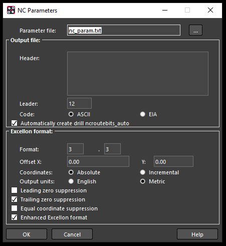
In addition to the above options, OrCAD works best with setting the following Parameters…. The format should have a precision of 3 before and 3 after the comma. The coordinates should be Absolute and Metric, and the Enhanced Excellon format should be selected. No zero suppression or one of the trailing or leading suppression should all work well.
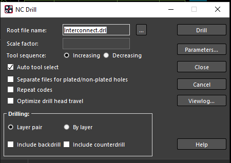
KiCad Drill settings
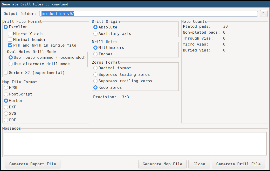
In KiCad, a similar result can be achieved by selecting the Excellon file format with PTH and NPTH in single file, an Absolute Drill Origin and Drill Units in Millimeters. In this case, the screenshot shows how to keep all zeroes, which will be the only structural difference to the file generated in Cadence with the options shown above.
Drill File: Further Readings
Bill of Materials
The Bill of Materials (BOM) is a spreadsheet that matches the component names from design with actual physical components. Both tools, Cadence and KiCad, can automatically generate these lists but might need some post-processing. Similarly to the drill files, there is no standard, but there are several recommendations and best practices. In general, *.csv and *.xlsx files are accepted, and we use both across the repositories.
Arguably the most crucial feature of a BOM is descriptive headers: the assembler will open the file and then try to match columns to the expected fields with as little manual intervention and margin for error as possible.
- ID, Item, or Line # (optional): unique row number
- Qty: number of components of this type
- RefDes: A single reference designator or a list of designators as used in the schematics
- Description: Generic description of part
- Footprint or Package: the components package
- Manufacturer (optional): Component manufacturer name
- MPN or Manufacturer #: Component manufacturer product number, e.g.,
RMCF0603JT220R. - [SUPPLIER]PN, e.g., DigikeyPN (optional): PN of a specific supplier, e.g., Digi-Key, Mouser, LCSC, for example,
RMCF0603JT220RDKR-ND - Notes or Instructions: Additional comments, for example, specify if it’s OK to use a generic component from the Description or determine alternatives to the suggested part.
The ID is optional but can help during the communication with the assembler. For example, you can say that “item 24 can be replaced by…” in an email. One way to provide alternatives for a part is to use additional letter indices; for example, ID 24a could reference C0603JR-07220RL, and ID 24b could specify RMCF0603JT220R. Use the Notes field to clarify this.
The RefDes should be a unique value for your design, often a letter followed by a number such as R1, C15, or U132.
The Description field can be used to describe the component. For example, a 220Ω resistor with ±5% tolerance, 100mW power, and a 0603 (1608 metric) package can be represented as 220 OHM, 5% 3/10W 0603. You should also generate a separate Footprint column, which can help identify the smallest package or the number of contacts if the assembly house requires that information.
It is generally helpful to name a particular component even for rather generic components like capacitors, connectors, or resistors. For that, specify the Manufacturer product number and since that might not be unique, give a manufacturer name of the company that produced this particular part. For example, you could stipulate the manufacturer Yageo and the MPN RC0603JR-07220RL.
If you know the supplier product number, you can specify it in additional columns. For example, the DigikeyPN could be 311-220GRDKR-ND, the MouserPN 603-RC0603JR-07220RL, and the LCSCPN C114683. Different assembly houses will use other suppliers and might prefer different component manufacturers for passive parts like resistors or capacitors. Columns for different suppliers can be added whenever needed or known. A good search engine to find electronic components and distributors is Octopart.
Finally, in the Notes, you can specify if it is OK to use the generic part from the description, which might be OK for resistors, but not for LEDs on the driver board. You can also use this column to specify alternatives; for example, alternative for 24a or if unavailable, use Stackpole RMCF0603JT220R or resistor matching description. You could even request if unavailable, get in contact if you have specific constraints for that part and want to be involved in finding an alternative. This is also the place to specify if components are consigned or if you are going to assemble them yourself.
Further Readings
- CircuitHub: New features to improve BOM workflow
- JLCPCB: Bill of Materials (BOM) File for SMT Assembly
- Bittele: Bill of Materials for PCB Assembly
- PCBWay: Files Requested for PCBA
Placement file
For board assembly, especially using SMT technology, a placement file is required. This file is sometimes called centroid file after its file format, Insertion, Pick’n’Place, or XY file. This file can be generated by Cadence and KiCad. Many assemblers can produce them from the Gerber files, but since this takes a long time and is an error-prone process, it is recommended to provide them.
The centroid format is a text-based file format, either as a fixed-width spreadsheet or column separation similar to a CSV. The file extension is often *.txt (Cadence), *.csv, or *.pos (KiCad) and recommendations are given in the IPC-7351B design document. A pick’n’place file contains the following columns:
- RefDes: unique designator
- Footprint (optional): Description of the package, e.g.,
0603R - Mid X or Location X: component’s X location
- Mid Y or Location Y: component’s Y location
- Rotation: component’s rotation
- Layer: Top or Bottom (or
T/B)
The RefDes is the same designator used in the design files and the BOM. Unlike the BOM file, there is only a single component per line in the centroid file.
The Footprint or Package column helps the assembler identify the best machine but is not considered essential as the information should be in the BOM.
The Location columns describe the components offset from the board origin. The board origin is the bottom left, as seen from the top side of the board. The units are given in inches. Usually, the center of the component is the reference for the placement, but for some parts like connectors or other off-centered elements, the reference is at a different location. Besides, some assemblers prefer the location of pin 1 as a reference. Some tools like Cadence will ask you which location you want to write to your centroid file. If in question, choose to provide the file with mid reference. There are instances where all three types are provided in the same file, then using Mid X/Y, Ref X/Y, and Pad X/Y as columns names. For some of the Modular LED Display fabrication files, we have provided all three types of pick’n’place files. Cadence calls these files body center.txt, origin.txt, and Pin1.txt.
The Rotation is a value in degree clockwise for parts on the bottom and counter-clockwise for parts on top.
The Layer specifies where the component is placed. Consequently, it also defines how the location and rotation are interpreted. An LED on the top with a rotation of 90 should have the cathode pointing down; the same LED with a rotation of 90 on the bottom side will have the cathode point upwards.
Further Readings
- PCBWay: Files Requested for PCBA
- Screaming Circuits: A few hints on the centroid file
- JLCPCB: Pick & Place File for SMT Assembly
Invoice
One topic that regularly comes up in conversations is the question about costs for a Modular LED Display. If you provide an estimate for the quote or invoice, we can add an anonymized version for outside labs. As there are huge differences between PCB manufacturers and over time, other labs can follow up on the most relevant information.
Please provide this basic information: The order date, a quantity, type of order (e.g., PCB manufacturer, assembly, parts order, or a combination of those), the price you paid, and if there is a difference, the initial quote you received. Some PCB manufacturers allow sharing projects publicly with a project ID, which will allow others to order the same item. If you have such an ID for the project, it can simplify future orders by sharing this identifier.
Further Readings
Feedback from the PCB manufacturers
Engineering and design are iterative processes that can be improved through feedback. The manufacturing process offers the chance to enhance the Modular LED Displays by improving issues that the PCB manufacturer’s engineers and systems find. Depending on the number of problems they have to fix on their side, PCB manufacturers might charge additional engineering fees. For one, it would be a waste to not use the information you paid for. And secondly, having to solve the same problems repeatedly for similar orders over time is a waste of time and other resources.
Not all PCB manufacturers provide feedback; sometimes, you have to explicitly ask for it. Also, the format, quality, and thoroughness of the feedback differ between PCB manufacturers, and not all problems can be generalized to other PCB manufacturers or assembly houses. Consequently, there is no simple recipe on how to use the input. Instead, here are a few examples of feedback and how this could become part of the next version.
Traces and routing
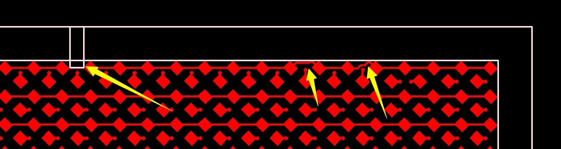
Depending on the machines the PCB manufacturer has at the shop, their process might be more sensitive to trace location, trace width, or distance between traces than the design software’s constraints. In this example, the two yellow arrows on the right point out that the traces come close to the edge. Since the margin of slack can be similar across different machines for different PCB manufacturers, and if there is no other downside, it might be worth considering to reroute these parts. This could require updating the design files and then regenerating the next batch’s fabrication files.
On the other hand, the arrow on the left shows a problem related to the panelization for this particular PCB manufacturer, where the exact location can not be generalized to other PCB manufacturers. Unless you want to engineer the panelization into the component’s design, this specific problem might not be worth considering for a general solution.
Other examples are the distance between traces: the design rule check (DRC) during the design might use a different constraint than the PCB manufacturer’s settings. Consequently, some traces might appear too close to each other or nearby a component. Suppose there is enough space on the board. In that case, it might be worth modifying that particular trace or even the rules in the design file instead of seeing the same error over and over across different PCB manufacturers. On the other hand, some PCB manufacturer might give feedback based on the requirements from their specific machines that are not generalizable. Furthermore, the work and risk of changing traces and pads when using differential pairs or same length traces, or when relying on impedance match might outweigh the benefit of improving the general design. This is just to mention, that there can be good reasons not to integrate the manufacturer’s feedback.
BOM corrections
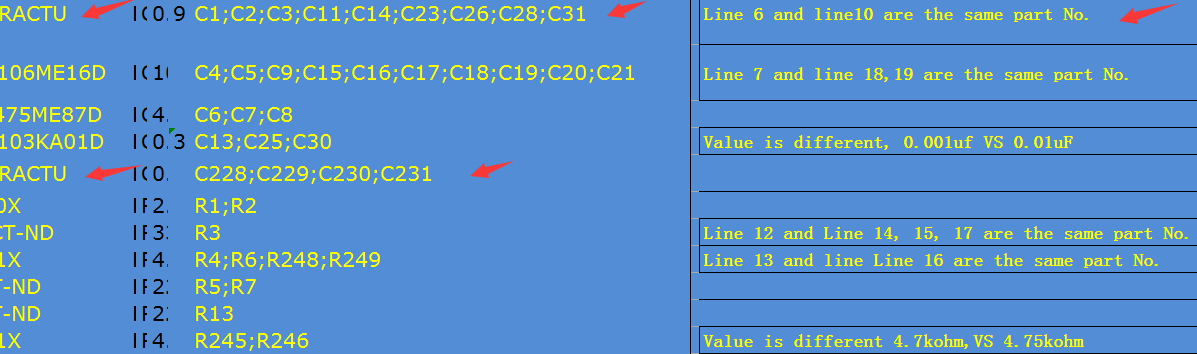
The automatic generation of BOM files through the design tools can lead to unexpected results. Suppose there is a small difference in a component’s specification, such as an additional space in the component description like 220Ohm vs. 220 Ohm. In that case, it can lead to duplicate BOM lines. Assembly houses bill per unique part, so reducing the number of lines in the BOM avoids potential problems and save money. In the example feedback on the right, an assembler has highlighted this particular problem for several lines, including the first, second, seventh, and eighth.
Some differences between the specified component and the description are minimal, or the context in which they are used makes it easy to find a replacement. Correcting the original design files can reduce the communication cycles for future orders. This will also prevent problems for cases where these differences actually matter, and a prospective assembler might miss that problem. Examples of this particular issue are shown in the above example for lines four and the last line.
Different suppliers use other product numbers, and different assemblers might get their components from various suppliers. Suppose an assembler identifies a problem with the product number. In that case, it might be worth checking if the column MPN really contains the manufacturers’ product number and not the id from a supplier. In the example on the right, the BOM accidentally had a Digi-Key product number in the MPN column in lines two, three, and eight. Besides, if an assembler suggests the product number from a different supplier, it might save you some time and confusion down the road if you add a new column, e.g., for MouserPN. You might not need it immediately, but if you have the files open anyway and work through it, why not reduce future work.
Always try to keep the description of the package in sync with the actual part number. In the above BOM, the items in lines six and seven were specified as 0603 packages, but the part number suggests that these are really 0402 packages. Wrong sized can lead to faulty orders and unexpected costs: if the smallest component is smaller than specified throughout the quotation process and can lead to unforeseen delays.
By adding an additional column for a supplier in the BOM, this potential problem can be fixed. If the footprint of a component changes and might influence the PCB itself or several generated files, including pick’n’place and BOM, this might require an adaptation of the design files.
Drill files
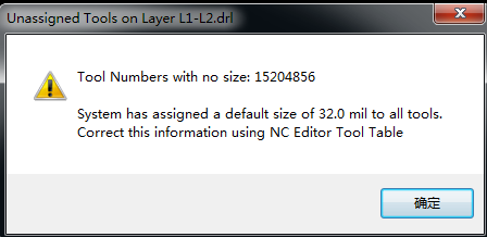
In the past, drill files were especially error-prone. This is possibly caused by OrCAD’s default settings that produce a non-standard file unless parameters are set correctly. In some instances, this is caused by missing configuration for the drill bit size in the header, as in the example screenshot of an error message that an assembler sent to us. Not all PCB manufacturers and assemblers will complain about all errors; they will assume a default tool size or copy drill bit size from an assembly file. This copy&paste process on the PCB manufacturer side adds a potential mistake to the PCB, which can easily be avoided by providing a valid drill file.
Since drill files are ASCII files, one way is to add the header information. “Further readings” in the drill file section provide some starting information on how to do this. In other cases, repeat codes caused the issue since not all machines support these newer file format features. While these issues can be fixed by editing the *.drl file as well, it is often easier to export another drill file following the suggestion in the drill file section.
Versioning
The file versioning loosely follows Semantic Versioning. Within a generation, the version number has two components, for example, comm-v0.3. This is an abbreviation for Modular LED Display communication board version 4.0.3.
Components are considered incompatible between generations; hence the generation acts as the “MAJOR” version.
Each component of the Modular LED Display follows its own “MINOR” versioning. For example, functional improvements on the arena board do not require changing the version of drivers or other components. Since many of a display generations’ repositories are independent of each other, the generation number does not need to be specified. Within the “Panels G4 Hardware” repository, the major version 4 is implicit, so that “version 0.3” automatically becomes 4.0.3.
Small changes, such as incremental improvements to design files or altered fabrication files based on the same design files, are acknowledged through the “PATCH” number. In the example above, version 4.0.3 is the 3rd patch of version 0 within generation 4 of the Modular LED Displays.
License
Files on the repositories are published under the CERN Open Hardware License weakly reciprocal version 2.0 (CERN-OHL-W) and/or the Creative Commons Attribution ShareAlike 4.0 International (CC BY-SA 4.0) licenses. If you require another license, send a request along with your submission.
Documentation
Different applications and knowledge require various emphasis within the documentation. If you figured something out that wasn’t documented before, then please consider contributing. Taking pictures during the hardware design and production is one of the things that are not essential but useful to have:
Renderings and photos
Visualizations help in identifying a version of a PCB or by documenting how it is used. When working on the design files, either Cadence software, as well as KiCad, supports the 3D rendering of the PCB. This image can be used to see the silkscreen that might otherwise be hidden after assembling a PCB. Once the PCB was produced and arrives, a photo can be used to document how it actually looks. This step is often not considered necessary during the design phase, and it’s certainly more exciting to try a new arrival than to take a picture.
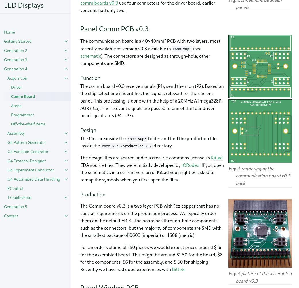
Having spent a lot of time trying to match actual hardware with descriptions and design files of different revisions, we assure you that creating these visualizations is well invested time (one example where this would have helped is the distinction between driver-v2.x and driver-v1.2). Especially since renderings in Cadence and KiCad are done quickly and once stored in the repository, they are always at hand when needed. Hopefully, the example shown on the right for the comm board can convince you to submit a rendering along with the files you sent to the assembly house. And the additional picture of the assembled boards will contribute to useful documentation.
How to contribute
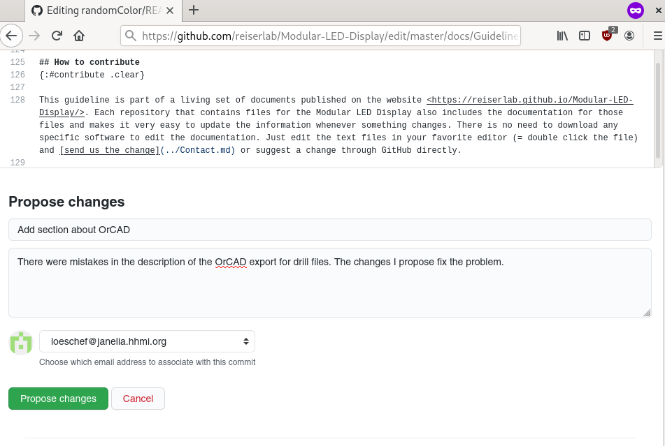
This guideline is part of a living set of documents published on the website https://reiserlab.github.io/Modular-LED-Display/. Each repository that contains files for the Modular LED Display also includes the documentation for those files and makes it very easy to update the information whenever something changes. There is no need to download any specific software to edit the documentation. Just edit the text files in your favorite editor (= double click the file) and send us the change or suggest a change through GitHub directly.
With the following steps, you can make a suggestion directly through GitHub:
Choose the file you want to edit on GitHub, for example, this guidelines_hardware.md
Click on the edit button with the pen icon, at which point you will be asked to log into GitHub (if you haven’t done that yet).

You can now change the file directly. Ignore the first few lines between --- and the second --- or learn more about it in the Documentation Guidelines. While editing the file, you can preview changes and then switch back to Edit file until you are happy with your changes. To save the changed version, write a short summary in one line and, if necessary, a longer description of what you did, and then click on Propose changes. This creates a copy of the file in your GitHub account, called a “fork” in git lingo. Let us know about your proposition and click on Create pull request.